Canatu - Specialist in Carbon Nanotube Films

I might have a slightly biased perspective on this case because I work with these things on a daily basis. However, I hope no one invests their hard-earned pennies based on my posts. I also research the semiconductor industry a lot in my free time, as I find it extremely interesting and educational, both professionally and from an investor’s perspective.

In my opinion, the narrative hasn’t gone anywhere. ASML’s machine power levels are increasing, and consequently, reticles require a pellicle made of a material that can withstand both the increasing power levels and hydrogen plasma.

The transition to new technology takes time, and that proverbial can has been kicked down the road in Canatu’s case. At the time of Canatu’s listing, I was under the impression that things were further along on the customer side, but now we have seen otherwise, and the share price is naturally following suit.

One must remember that the one reactor currently in the field hasn’t yet achieved an approved SAT (Site Acceptance Test), which might partly explain the share price reaction. The market may be afraid that the project won’t succeed and that the customer will choose a supplier like Mitsui instead. My strong guess is that this unnamed customer is TSMC.

Canatu’s new management has also been pressed on what is required to get the SAT across the finish line with this customer as well. The answers have been very political: “We need cooperation, and we believe we will get it across the finish line soon.” I might be completely wrong, but it could be that TSMC wants to validate a broader package that includes the pellicle supplied by Canatu and a (new EUV) reticle, as well as certain process-related conditions. Only when everything is successfully validated will Canatu’s SAT be approved. In this case, Canatu’s process would be fine, but given Canatu’s limited muscle, they simply have to settle for the conditions set by TSMC and accept the aforementioned process. Or then, it could be that Canatu’s own process still needs some fine-tuning before TSMC can approve it. However, since Canatu has already been refining its process for several years with both IMEC and ASML, I’m somewhat leaning toward the first option, where approval is tied to other parameters. I intend to seek confirmation on these points at the spring AGM at the latest.

It must also be remembered that Canatu does not hold a monopoly position like ASML, for example. Mitsui and Lintec are working to gain market share, and this certainly explains part of the share price decline as well. However, FST and potentially TSMC are very strong references looking into the future.

Based on my own research, however, Canatu has certain strengths compared to its competitors Mitsui and Lintec. One of these is dry deposition technology. Other strengths include high 13.5 nm transmission, which, as I understand it, is a few percentage points higher than competitors’. But this is inherently a very critical parameter, as ASML’s machine produces more wafers the more light can be directed onto the silicon wafer.

As for the questions from user @123456789, I think they contain quite a bit of AI hallucination.

1. TSMC certainly manufactures pellicles in-house because they have their own “mask shop”, but they purchase the technology from someone else. TSMC definitely does not want to tie up its own R&D budget on something it can buy for pocket money from an external supplier.

2. This is true, but pellicles do not last forever. In addition, every reticle needs its own, and the more complex the manufacturing process becomes, the more reticles are needed. Sure, the future 6 x 12 reticle will solve some current issues, so the total number of reticles might not grow as much. However, that is still a long way off, and anything can happen before then.

3. A pellicle-free process is not an option. :smiley:

36 Likes

It’s ugly out there in the stock market when shares are being dumped indiscriminately. I bought more yesterday, but naturally, I could’ve gotten them much cheaper today :frowning: The only downside to this downhill slide is that I can’t raise cash as fast as I’d like. If you roughly extrapolate the stock price, it’ll hit €0 in about six months. Luckily, insiders have also been loading up, so we’re in the same boat with the company’s management and can share our frustration over the melting of our holdings at the AGM.
6 Likes

Now the market cap is down to just 134 million.
You get 20 years of R&D with over 100 million in investments for cheap.

3 Likes

The ongoing unwinding of the AI trade certainly adds downward momentum to the share price, but it’s still quite strange that there’s no buying pressure to be found anywhere and the price is just allowed to drift down freely. We’re truly approaching a special situation soon where the market assigns zero value to the company’s technology, patents, and contracts.

7 Likes

Thank you very much @Pandakarhu for the answers!

Regarding point 1, I slightly disagree; large corporations are often more than willing to take business from smaller players, and a typical move would be to pry into the technology under the guise of cooperation and then coldly take advantage of the situation once the patents expire. It certainly wouldn’t be the first time.

Regarding point 3, I could hardly believe this claim made by the AI myself. I questioned it several times. Here is more explanation: "Yes, this is true, but only in EUV. In conventional DUV lithography, pellicles are standard equipment for everyone. To clarify my previous phrasing: it’s about Samsung not having used EUV pellicles in high-volume production, not that they have never tested them.

What happened. When EUV entered production in 2018–2019, viable pellicles didn’t exist yet, so TSMC and Samsung developed methods to run EUV scanners without a protective membrane. As early as 2017, Samsung estimated that without a pellicle, the wafer scrap rate could be kept below two percent even if the mask gets contaminated. anandtechcadence

Samsung planned deployment starting in 2023, with the rationale being that pellicles achieving over 90% transmission had not been previously available. However, by April 2023, they had not yet deployed them, with the suspected reason being concerns that pellicle damage could halt the entire production line. Therefore, the Taylor 2 nm fab marks the first real volume production deployment. thelecthelec

How they manage without a pellicle. The mask must be regularly inspected for particles adhering to the patterned area, and every inspection reduces monthly wafer output. Additionally, wafers are inspected immediately after exposure: if a defect is found, the photoresist is stripped and the wafer is re-exposed. It is a balance between inspection costs and yield risk. Substackanandtech

TSMC’s situation appears contradictory across sources. According to a Korean publication, TSMC has been gradually adopting Mitsui’s pellicles since 2019. According to another source, TSMC reported as late as 2023 that its pellicle infrastructure had just been completed but was not yet in production. In all likelihood, adoption has been layer-specific and limited. Substack

Significance for Canatu. This cuts both ways. It proves that pellicle-free production is an economically viable alternative, meaning the adoption of CNT pellicles is not a given. On the other hand, it means that Samsung’s transition to pellicles represents entirely new demand, not a redistribution of the existing market. The sources are partly Korean industry press, so the exact layer-by-layer adoption rate cannot be confirmed from public sources." Well, I really doubt that this isn’t true.

Could it also be that investors are more interested in companies that are already turning a profit and growing profitably… For Canatu, that seems to be two years away at best, and even then, only maybe. If you think Canatu is the absolute best place to put your money right now, then you should buy, but otherwise, there’s good reason to look elsewhere and sell any shares you might already own.

3 Likes

Even Atte agrees with the forum’s hive mind, though it might not be quite what it used to be. Oh well, Hesuli is Hesuli!

34 Likes

SÄ knows how to give good feedback on technology. In short, Canatu’s technology is better, but Mitsui has been an ASML partner for a longer time and Intel relies on Mitsui. Canatu, on the other hand, collaborates with the South Korean ecosystem.

It is indeed good to monitor what the competitor is doing from time to time. Canatu should invest more in end customers so that they don’t settle for a mediocre solution for lack of a better option.

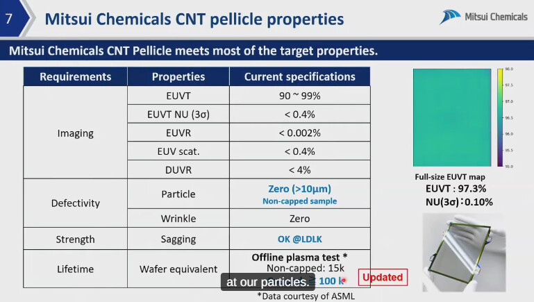
Intel acts as a critical end-user, validator, and co-developer within the EUV ecosystem that relies heavily on Mitsui Chemicals’ pellicle pipeline. Rather than an exclusive supplier-buyer dynamic, their relationship is structured around multi-party alliances designed to push the limits of advanced logic chipmaking. [1, 2, 3, 4]

The connection between Mitsui and Intel is broken down into three key pillars:

1. The ASML-Imec Validation Bridge

Intel does not typically negotiate raw pellicle development completely in isolation; instead, it operates through ASML and imec (the Belgian nanoelectronics hub). [1, 2, 3]

  • The Route: ASML originally licensed its fundamental EUV pellicle design and assembly technology to Mitsui Chemicals.
  • The Role: As Mitsui builds out its mass-production facilities (such as the 5,000 sheets/year facility at Iwakuni-Ohtake Works), Intel utilizes its position as an imec core partner to test and validate Mitsui’s standard silicon-based and upcoming Carbon Nanotube (CNT) pellicles on pilot lines. [1, 2, 3, 4, 5, 6]

2. High-NA EUV Integration (The 0.55 NA Frontier)

Intel pioneered the industry deployment of ASML’s next-generation High-NA EUV systems (the EXE:5200 series scanners). High-NA introduces unique mechanical constraints:

  • The Challenge: High-NA features a narrower field size and a much steeper light angle of incidence, requiring specialized pellicle geometry to prevent clipping the EUV beam. [1]
  • The Collaboration: Intel works alongside ASML and Mitsui to run comparative evaluations on these pilot exposure systems. Mitsui specifically targets its CNT product pipeline to fit these exact High-NA requirements. [1, 2, 3]

3. High-Power Scaling Roadmap

Intel’s aggressive power roadmap for its advanced nodes targets scanner source power levels scaling toward 600W and up to 1kW+.

  • Because Intel pushes scanner output so aggressively, they are a primary driving force behind Mitsui’s shift from traditional silicon-based pellicles to CNT membranes. [1, 2]
  • Intel requires pellicles that can withstand intense thermal cycles without deformation, directly steering Mitsui’s R&D focus toward long-term membrane endurance under intense exposure. [1, 2]
5 Likes