DNP is teaming up with Rapidus. I’d guess that this business will go to the Mitsuis. All three are Japanese players.
6 Likes

In that image are the ASML High-NA and Low-NA (upper) roadmaps that I have occasionally referred to. Let’s save it here since it was shared publicly. This image is significant for the future.
In the ASML roadmaps (paid version, not this image), there is indeed support/use for the CNT pellicle from the NXE:3800F model onwards. The timing matches what CEO Kokkonen has been talking about.
16 Likes
[Exclusive] Samsung Taylor Fab Mass Production of Semiconductors Delayed to Next Year
Mass production at Samsung Electronics’ Taylor plant, once expected as early as this year, has been pushed back to early next year, according to multiple sources with knowledge of the matter.
The shift in the schedule could impact Tesla and other potential Big Tech clients after the Korean chipmaker nabbed multibillion-dollar contracts to manufacture chips utilizing its latest 2-nanometer process.
“It appears that even internally at Samsung, the timeline for the start of mass production has not yet been finalized,” a source familiar with developments told the Korea JoongAng Daily. “The schedule has continued to slip, and it is now understood that a full-scale ramp-up for a meaningful volume output could be pushed to early next year.”
Another source at a semiconductor materials firm echoed the setback.
“The plant has begun pilot operations, but full-scale manufacturing has already been significantly delayed,” the source said. “The timeline appears to shift frequently, and there is no clear start-of-production milestone,” he said, adding that there appear to be factory utilization issues without specifying further.
The change in the timeline comes as a surprise, given earlier expectations that production ramp-up would begin by the end of this year. During its January conference call, the chipmaker said that the foundry process for its second-generation 2-nanometer chips, also known as SF2P, was set to enter mass production this year, which many took to refer to a ramp-up at the Taylor site.
“For 2-nano, we expect our first-generation mass production to further stabilize, and we are working to secure manufacturability and develop design infrastructure for the second-generation process targeting mass production in the second half of the year,” Kang Suk-chae, executive vice president of Samsung Foundry, said in January.
Samsung also projected on-year growth in 2-nanometer orders of more than 130 percent this year, driven by the production of high-performance computing and AI chips on its second-generation 2-nanometer process in 2026.
The 2-nanometer process is to be developed at both the Taylor site and its Pyeongtaek campus in Gyeonggi, but facilities at the Korean site are still under construction, and those originally planned as a foundry line have since been switched to focus on expanding memory production to meet surging AI-driven demand.
Analysts believe that the large-scale production of Samsung’s SF2P will mainly take place at the Taylor site due primarily to better accessibility to major target clients, while the Korean facilities are responsible for sample production in the early stage.
Multiple reports said that Samsung Foundry is in talks to secure major orders from Big Tech firms including Google, AMD and more recently, ByteDance.
A Samsung Electronics spokesperson clarified that references to the start of production should be understood as the completion of preparations for mass manufacturing by the end of 2026.
“The plant will be ready to be operational by then,” the spokesperson said.
Since 2025, Samsung has maintained that production at its Taylor site will begin in the second half of 2026, with construction moving forward as planned following earlier delays. The latest developments suggest the company may be drawing a distinction between the start of production and full-scale mass production.
Confidence in the 2026 mass production timeline strengthened after the company secured a $16.5 billion contract with Tesla to manufacture AI6 chips in July of last year. Elon Musk later said the chipmaker would produce a portion of AI5 chips as well.
Samsung has already begun limited activities at the site after acquiring a temporary certificate of occupancy from the city of Taylor covering approximately 88,000 square feet at Fab 1. Trial operations, including tests of its extreme ultraviolet lithography equipment, are reportedly set to begin this month.
First announced in November 2021, the Taylor project has faced multiple delays, prompting the Texan city to add a clause on stricter timeline checkpoints to keep construction on track, setting a goal for Samsung to complete a total of 6 million square feet by 2026, with an additional 1 million square feet to be added by 2028.
Signs of progress are nevertheless emerging: The company has recently opened 180 job positions at the site, spanning facilities and infrastructure build-out, tool installation and equipment readiness, as well as yield engineering and manufacturing support. Applications for these roles will be accepted through Dec. 31.
Musk previously stated on X that mass production of the AI5 chip is expected around mid-2027.
A third source told the Korea JoongAng Daily that a clearer production road map could emerge by June.
“Based on public information, the facility itself is not particularly large — roughly half the size of one of Samsung’s Pyeongtaek lines — and it is dedicated entirely to foundry production,” the source said. “Regardless of the pace of ramp-up, production is expected to begin this year. Major equipment installations are anticipated around March or April.”
7 Likes
Read this morning’s announcement here:
Inside information: Canatu Oyj abandons its long-term financial targets
Canatu Oyj (“Canatu”) announced its long-term financial targets in the company prospectus published in August 2024, prior to the initial listing of Canatu’s shares on the Nasdaq First North Growth Market Finland marketplace. These long-term financial targets were to achieve revenue of over EUR 100 million and an adjusted operating profit margin* of over 30 percent in 2027.
11 Likes
Here is some reading and food for thought for the morning. Financial statements:
July–December 2025 in brief*
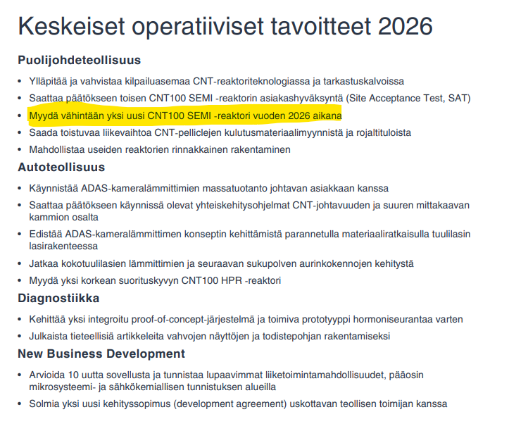
- The first customer-approved CNT100 SEMI reactor and related post-processing equipment were licensed, marking a step towards the commercial adoption of CNT pellicles
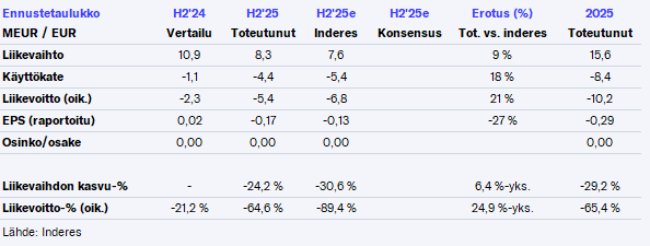
- Revenue decreased by 24.2% to EUR 8.3 million (11.0)
- Gross profit decreased by 7.4% to EUR 6.4 million (6.9), or 77.0% (63.0%) of revenue
- EBITDA was EUR -4.4 million (-1.9), or -52.5% (-17.2%) of revenue
- Adjusted operating profit was EUR -5.4 million (-2.5), or -64.4% (-23.2%) of revenue
- Operating profit (loss) was EUR -5.6 million (-2.8)
- Basic and diluted earnings per share were EUR -0.17 (-0.03)
- The average number of employees (FTE) was 157 (130), and the number of employees at the end of the reporting period was 181 (137).
January–December 2025 in brief*
- Revenue decreased by 29.2% to EUR 15.6 million (22.0)
- Gross profit decreased by 17.9% to EUR 11.3 million (13.8), or 72.5% (62.5%) of revenue
- EBITDA was EUR -8.4 million (-3.6), or -53.9% (-16.1%) of revenue
- Adjusted operating profit was EUR -10.2 million (-4.8), or -65.3% (-21.9%) of revenue
- Operating profit (loss) was EUR -10.7 million (-5.3)
- Basic and diluted earnings per share were EUR -0.29 (-0.05)
- The average number of employees (FTE) was 145 (123), and the number of employees at the end of the reporting period was 181 (137).
And then a follow-up order:
Canatu has received a follow-up order for long lead-time components from an existing CNT100 SEMI reactor customer
Canatu Plc, a deep technology company developing advanced carbon nanotubes (CNT), has received a follow-up order from its long-term global semiconductor customer. The order consists solely of long lead-time components and related preparatory work concerning the design, manufacture, and potential procurement preparation of parts that could be used in a potential second CNT100 SEMI reactor for the customer.
11 Likes
Canatu emphasizes the slowness of the market transition, but based on the comments, there might be hiccups with their own product as well.
There have been delays in the process that have affected the progress of customer approvals and the timing of follow-on reactor orders for existing customers, but the process is still moving forward.
The decline was mainly due to slower-than-expected progress in customer approvals, which delayed revenue recognition as well as follow-on reactor orders from existing customers.
Estimating the timing of growth is exceptionally difficult for an investor — or impossible, when the company itself seems to be quite in the dark about how the situation is developing.
In accordance with its disclosure policy, Canatu does not provide numerical financial guidance for the 2026 financial year.
- In the short term, Canatu sees several factors that weaken revenue predictability and increase volatility in the semiconductor and automotive industries.
- Canatu has ongoing customer negotiations, the timing and outcome of which are uncertain.
- For example, the commercial rollout of finished CNT pellicles ultimately depends on the processes and schedules of Canatu’s customers.
- The schedule for the customer approval (SAT) of the second CNT100 SEMI reactor is not fully within Canatu’s control, which is why the risk of delays cannot be ruled out.
Approvals are taking a long time.
At the same time, the customer approval process (SAT) for the second CNT100 SEMI reactor, delivered to a leading global semiconductor player in December 2024, is ongoing, and the schedule is partly affected by the customer’s own progress.
I would love to own this company, but I’m really wondering how much cheaper it could potentially be bought for compared to the current price. Not a single word seemed to be said about new reactor orders.
Edit. Dropping the financial targets at least confirms that they won’t be achieved. Of course, this wasn’t a very big surprise at this stage. The CMD at the end of the month will be interesting.
9 Likes
Whew, there was a lot of info in the report, and I’ll return with a more detailed breakdown as usual in tomorrow’s update. H2 figures were slightly better than my expectations, but this doesn’t have such a significant impact on the case.
No numerical guidance was provided for this year, as there are so many moving parts and uncertainties. In light of these operational targets, the sale of two reactors I projected for this year is not yet set in stone. Well, naturally this year’s growth won’t settle the investment story yet, but waiting for growth is never pleasant.
The long-term growth outlook still looks good, and our expectations for the case’s true realization are weighted towards 2028-2029. Giving up the financial targets was no longer a surprise, as the growth can was unofficially kicked for these already in the H1 report. I need to ask more about those delays today—whether they refer to the delays seen in the early part of last year or if much more has happened recently. As mentioned above, this month’s CMD will be interesting!
33 Likes
I need to ask more about those delays today—whether they refer to the delays already seen in the early part of last year, or if there have been many more very recently.
If you could also challenge the CEO on whether there have been any issues with their reactor or other complications regarding customer commissioning, rather than just market-related factors behind the slowdowns. Some of the wording in the report was a bit vague in this regard.
15 Likes
The 2026 outlook looks uncertain based on the actual earnings release. Inderes will likely have to lower its estimates for the current year (assuming 1 reactor instead of 2). On the other hand, the “risk” that no reactors would be sold seems slightly smaller; Samsung has clearly requested preparation for the next reactor and will likely order it later.
I could be wrong, but Samsung’s intention is hardly to “string along” small subcontractors by making “pre-orders for LLI products” and then failing to follow through. This also has positive signaling value.
Canatu is a growth company, and even though today’s [reaction] might be deserved in Mr. Market’s opinion, I think the most important part of the announcements can be found in the CN100 pre-order release:
Growing demand for advanced chips continues to drive the adoption of high-power EUV scanners and CNT pellicles. Production of advanced chips with 600-watt EUV scanners is expected to begin during 2027, which is estimated to be a turning point for the potential wider adoption of CNT pellicles.
Yeah, wide adoption isn’t exactly a done deal, but personally, I’m investing in this specifically in the hope of that. Looking forward to hearing more in the webcast.
Edit. Intel’s customer negotiations regarding 1.4nm High-NA production will be interesting to follow this year. We’ll certainly be wiser about the customers by summer/autumn. Over there, using CNT pellicles is mandatory, and it will be interesting to see if the contract goes to Mitsui or Canatu.
5 Likes
As a reminder, semiconductor industry equipment is not among the simplest, and delays and process fine-tuning at the customer end are more the rule than the exception in the semiconductor industry. I can say from my own experience that in many semiconductor equipment projects I have been involved in, there has always been some kind of delay or accumulated backlog. So, I wouldn’t say that the product has hiccups; it’s just part of the normal validation process.
Forecasts will indeed have to be lowered slightly again; in my own projections, no reactors will be delivered this year, though I would gladly be wrong about this. The focus now turns primarily to what the company comments regarding the commissioning of the current reactors.
17 Likes
Can you comment on roughly how long the commissioning processes could be? Currently, the approval process for the reactor delivered in December 2024 is still ongoing after ~15 months, and apparently to a significant extent, as nothing has been said regarding the completion of the process.
Second question: can you estimate how much the commissioning of potential subsequent reactors could be accelerated once the specifications for the first one have been established?
2 Likes
I totally agree. Yes, the cancellation of the financial guidance for 2027 is not particularly optimistic. However, it is important to understand the complexity and demanding nature of the entire semiconductor industry. There are only a few key players here, and they must ensure a fully secure, reliable, and stable environment for their future next generation manufacturing operations. As a result, all necessary approvals simply take longer than originally expected. This is not especially surprising.
That said, I expect the management to promptly establish updated guidance and plans to ensure transparent communication with investors.
1 Like
I still don’t understand why Canatu only supplies reactors and not the pellicles themselves. It doesn’t make much sense in the long run to remain a raw material supplier, does it?
Furthermore, a significant number of people have joined the company, but the results are lackluster. Has the hiring actually been successful?
1 Like
I can comment on a very general level, as I don’t know the exact details of Canatu’s technology. Projects are generally divided into the following phases:
- Equipment installation; the equipment is physically installed at the customer’s site. Typically, this takes 6–12 months.
- Process ramp-up and optimization. Typically 6–12 months. This phase is usually not carried out simultaneously with phase 1.
- First test batches; these are conducted in parallel with phase 2. It is very difficult to provide any estimates for this, as it depends heavily on the process. This continues until the customer is satisfied with the product or the primary point defined in the specifications is reached.
- Usually, the customer wants the device to be connected to an existing interface within the FAB. There can be several of these, such as SECS/GEM, various process data integrations, device loading, etc. These can also easily add up to several months of work.
This outline is very rough and should not be used as a direct conclusion regarding Canatu’s CVD chamber.
12 Likes
A few takeaways from the webcast regarding the semiconductor industry (Free Q&A translations noted below):
-
Reference to the early-year SPIE conference and the Beryllium presentation (a reference to the SPIE presentation was mentioned here earlier): “It is known that Beryllium is extremely toxic, and there was clear reluctance to introduce such material into EUV tools. We will continue with CNT pellicles for as far as we have visibility ahead.”
-
Competitive situation: “Lintec hasn’t gained traction in the market so far, even though they developed their own solution. They were the ones who called and asked us for reactors (last year). As for Mitsui, they are using an uncoated CNT pellicle, so its durability cannot match Canatu’s. Therefore, Canatu’s market position in CNT pellicles is ‘very competitive’.”
-
“First license fees from CNT100 production are coming from a customer this year.”
-
Confirmation that CNT pellicles are needed from 600W levels regardless of whether it is Low or High-NA.
-
“Canatu is also used in 2nm production / sub-600W production” (my own interpretation: This, in my opinion, confirms that for Samsung, it’s about the starting Low NA production this year at the Taylor Fab).
-
Timont’s own question: “Foundries are showing high interest in Low NA 600W tools regarding pellicles. The entire industry (ASML) is welcoming CNT pellicles with ‘great enthusiasm’. This allows for more power to be extracted from these tools. From ASML’s side, they have come to thank Kokkonen for having this solution available.”
In my opinion, this technical side still looks really good. Just have to wait for the nodes to progress. strong hodl
31 Likes

signs
13 Likes
Here is a company report on Canatu from Atte regarding the H2 results. ![]()
We reiterate our Add recommendation for Canatu, but lower the target price to EUR 9.0 (previously EUR 10.0). The company’s loss for the end of the year was slightly smaller than our expectations, but our forecasts have decreased based on the outlook comments for 2026. Following last year’s weak performance, a clear dent has appeared in the company’s growth story, which is also reflected in the share price. Nevertheless, the market for Canatu’s CNT-based pellicles is still forming, and the company’s position here appears strong. Canatu’s long-term potential thus remains attractive, but investors are required to have patience, which is being put to the test.
7 Likes
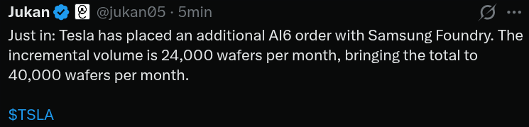
Exclusive: Tesla to “More Than Double AI6 Production”… Pursuing Additional Orders with Samsung
Summary
Tesla has been identified as being in discussions with Samsung Electronics to expand production volumes of its next-generation artificial intelligence (AI) chip. The two companies are reportedly at the stage of negotiating additional orders on top of existing contract volumes.
According to industry sources on March 4, senior Tesla procurement officials are scheduled to visit Samsung Electronics this week to discuss expanding foundry production volumes for the 2-nanometer next-generation AI chip, AI6. Tesla is understood to have already communicated its request for additional volumes to Samsung Electronics ahead of this visit. The volume contracted last year was approximately 16,000 wafers per month on a wafer-input basis. The additional volume Tesla has requested is roughly 24,000 wafers. This visit is intended to negotiate specific supply terms based on that request. If the deal is finalized, total production volume would increase to approximately 40,000 wafers — a volume that could significantly contribute to securing initial utilization rates at Samsung Electronics’ foundry fab currently under construction in Taylor, Texas.
Tesla previously signed a foundry contract with Samsung Electronics last year for AI6 chip production. At the time, the contract covered a supply period through December 31, 2033, with a contract value of approximately KRW 22.8 trillion. Given the eight-year long-term nature of the contract, analysts interpreted this as implying KRW 2–3 trillion in new annual revenue. Because the additional volumes now under discussion exceed the original contract volumes, the additional contract value is expected to be even larger.
The AI6 chip is reportedly intended for use across multiple Tesla platforms. Industry observers expect the chip to be deployed not only in vehicle autonomous driving systems but also in the Optimus humanoid robot and Tesla’s own AI data centers. The AI6 cluster is expected to take over the role of Dojo, Tesla’s in-house AI supercomputer that was effectively shelved last year. Industry sources believe it will be operated in a cluster configuration, with multiple chips grouped on a single server board.
Tesla has recently been ramping up AI infrastructure investment significantly to advance its autonomous driving services and robot development. During its January earnings call, Tesla stated that “this year’s capital expenditure will expand to a record level exceeding approximately $20 billion.” This is roughly double the recent annual investment range of $8–11 billion.
Samsung Electronics’ semiconductor partnership with Tesla dates back to 2019. At the time, the System LSI division participated in ASIC design while the foundry division produced the chip on its 14nm process — that product was HW3 (AI3). HW4 (AI4), currently installed in vehicles, was also produced on Samsung’s 5nm process. While Tesla split AI5 production between TSMC and Samsung, it has decided to place AI6 production back with Samsung.
Tesla is pursuing a so-called “No China, No Taiwan” strategy with its major component suppliers. The company has already openly communicated this strategy to module partners, urging them to exclude components from those regions. This is a strategic move to eliminate supply chain risks for core components, including semiconductors, amid escalating U.S.-China tensions and Taiwan Strait risks. Samsung Electronics’ Taylor fab, a leading-edge process facility located in Texas, aligns precisely with this strategy.
Once these additional order negotiations are concluded, Samsung Electronics’ foundry division will have secured substantial volumes at leading-edge nodes. An industry official commented, “While final confirmation and detailed production schedules remain subject to change, if this deal goes through, it would serve as a powerful catalyst for a turnaround in Samsung Electronics’ foundry business.”
The partnership between the two companies extends beyond semiconductor manufacturing. Samsung Electronics’ System LSI division has completed development of a 5G vehicle modem for Tesla and is set to begin supply in the first half of this year. Initial volumes are expected to be applied to Texas robotaxis before expanding to general vehicles. The scope of collaboration between the two companies continues to broaden.
As I understand it, this AI6 is precisely the product that Samsung will be manufacturing at the Taylor Fab on a 2nm / 500W line using Canatu pellicles. These kinds of additional orders could serve as a good catalyst for the need for a second reactor.
Speculation: There are many variables, but next year with a production volume of 40k wafers (AI6 alone), one could roughly estimate that 8 NXE:3800E units would be needed in continuous production (24/7), which would push total monthly pellicle consumption over a hundred units (assuming a conservative 10k exposures per pellicle). Depending on other parameters estimated, royalties could easily exceed €500k per month. Let’s say a guess of 5–7 million on an annual level from '27 onwards.
15 Likes
A small nuance regarding the pellicle price:
-
In the earnings webcast, Kokkonen spoke about composite pellicle prices ranging between ~$35-50k. He also implied that CNTs are ‘of course more valuable’, etc.
-
In previous news (01/2026), it was reported that the internally produced pellicles for Samsung’s use would be in the >35k€ price range (estimate). This would fall into that composite category (30-43k€ in euros).
Accordingly, it is expected that the introduction of domestically produced EUV pellicles will have a significant impact on the equipment and parts industry. The price of the EUV pellicle is estimated to be more than 60 million won.
I wonder if there was a slip-up by Kokkonen here? Looking at public sources, EUV pellicles have previously been in the maybe $10k price range, and they are indeed now expected to rise to that upper range I mentioned.
- Perhaps he accidentally let his own price range slip out; or
- alternatively, Canatu really intends to sell super expensive pellicles (e.g., $50-100k?). I believe the former is more likely.
6 Likes
Intel’s CFO reiterated that the company remains aligned with its original roadmap. Under the current plan, 14A is expected to enter risk production in 2027, with volume production targeted for 2029.
Canatu’s upcoming roadmap update will likely reflect Intel’s and TSMC’s 1.4nm production to some extent - although the presumed negotiations with Intel are still in progress, so there is uncertainty in that regard. One bonus reactor is a strong possibility (for Intel) by the end of the year if a deal is reached.
If the roadmaps don’t change significantly for the worse, quite a lot should start happening in 2028-2029. In 2027, the initial pace will be ramped up with Samsung.
5 Likes