What is the difference between warrants and subscription rights, the so-called “merkkari”?
Is additional money used for warrants in the same way as when exercising subscription rights?
What is the difference between warrants and subscription rights, the so-called “merkkari”?
Is additional money used for warrants in the same way as when exercising subscription rights?
A bit like a small, personal rights issue where you have the right to subscribe for shares at a certain ratio based on your own holdings. You can also sell this right.
In other words, you have to use real money if you want to exercise the warrants.
I’ve been doing some fundamental research on Canatu’s business idea for a few hours, and at first, I had great difficulty understanding the company’s business—and I’m surely not the only one. So, I thought I’d share my findings here with other investors in plain language, so that everyone can understand where this company will be getting its money from.
In everyday life, we encounter many situations where different types of transparent films are needed:


But what if these familiar products aren’t enough, and something stronger and more durable is needed?
For example, in microchip manufacturing, the silicon wafer is illuminated with EUV light, and a film (Pellicle) is needed in between to let the light through while keeping impurities away:
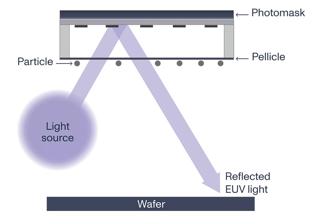
The challenge here is that the monopoly machine manufacturer, ASML, must use increasingly powerful light sources in its new technological processes. Because of this, current film solutions struggle to withstand the intense light and the heat it generates, which forces a slowdown in production. One ASML machine costs 200–500 million euros, and the demand for the most high-end high-tech chips is massive as the AI boom gains momentum, so even small efficiency gains are critical for the manufacturer.
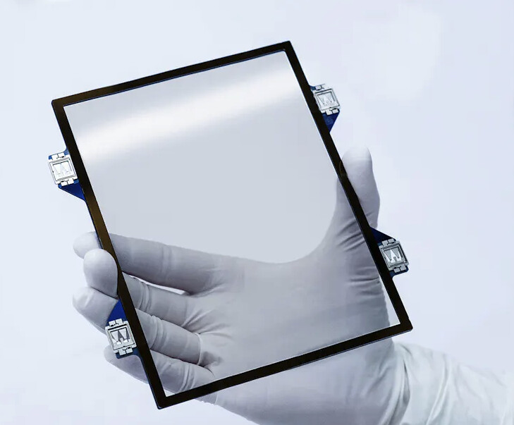
One possible solution to this problem is the carbon nanotube films manufactured by Canatu (Carbon nano tube), which possess extremely good properties:
The world is full of different applications where films need the ability to function in extreme conditions. For instance, when filming X-rays with a telescope in space, you need something stronger than plastic wrap. Canatu has, among other things, worked with the European Space Agency (ESA) to research what kind of films should be used in space sensors in the future:

One clear area of growth in the coming years is the number of sensors in cars. Soon, self-driving capabilities will be standard in every car, and they need to be able to drive in all kinds of weather. Anyone who has used a parking sensor in winter knows how easily snow and ice interfere with its operation, and soon there will be a vast number of these sensors all over the car. A Canatu film can be placed on lenses or, for example, in front of a LiDAR (laser scanner), through which electricity is conducted. As we remember from basic physics, electricity can easily be converted into heat, thus keeping the car’s sensors functional even in difficult weather conditions:

Less known in Finland, but the massive company Denso is one of Canatu’s partners in this field:
https://fi.wikipedia.org/wiki/Denso
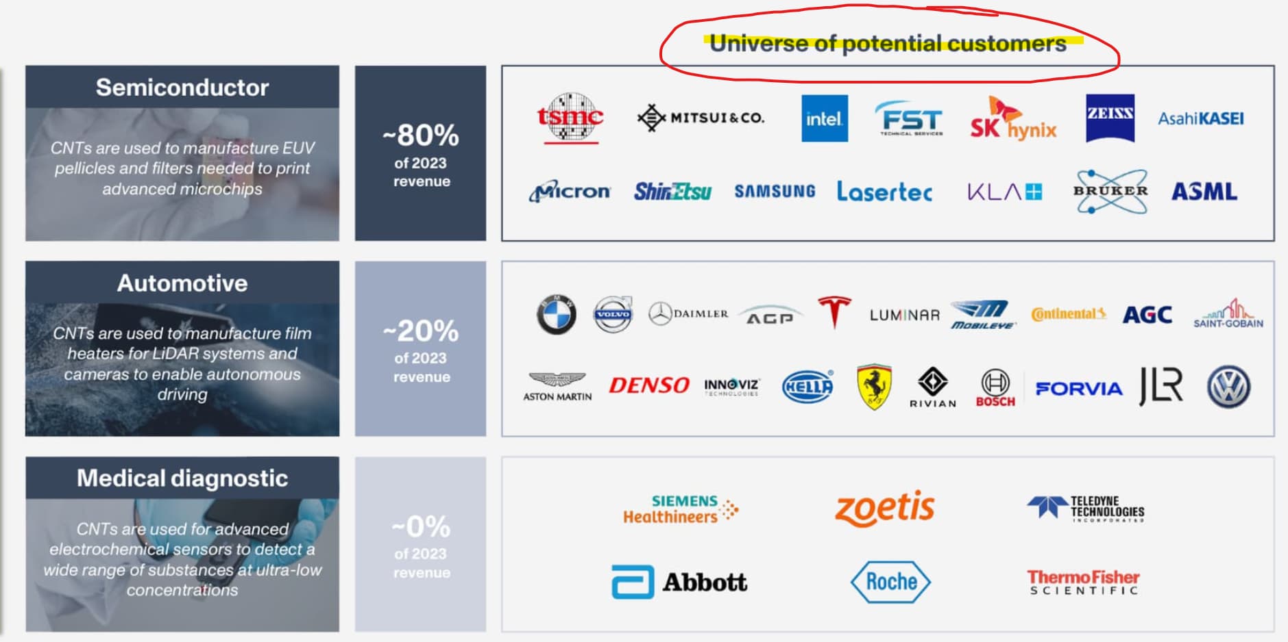
Canatu is exploring many other potential uses for these carbon nanotube films, such as electrochemical biosensors made from them for medical use and other similar interesting opportunities. However, the semiconductor industry and the automotive industry will certainly be the areas where the most lucrative customers will be found in the coming years, with all other applications likely moving toward the 2030s.
It probably doesn’t make sense to manufacture all the world’s carbon nanotube films in Vantaa, so Canatu also develops, produces, and licenses these film machines, called reactors, to other companies. In plain language, a reactor is a device or vessel where chemical reactions take place—meaning one substance is transformed into another. In practice, carbon-rich gas is fed into the top of the reactor, and through reactions, carbon atoms are made to combine into long chains (tubes), which are layered into a thin film at the bottom of the reactor. These then undergo some kind of post-processing, after which the film is ready:

Canatu also sells services and spare parts for these reactors licensed to customers, which could enable rapid and very capital-light growth. The market is only just taking shape in the coming years, so it is still unclear whether the company should be a film manufacturer, a film machine manufacturer, or perhaps both as it matures. At this stage, it obviously makes sense to take all the profitable growth available in the market.
Canatu holds just under two hundred patents, but despite the high technology, they won’t be operating alone in the market. Competitors include at least Mitsui and Lintec, and at this stage, it is still far too early to say who has the best technology or, on the other hand, who is the best sales powerhouse. I warmly welcome Canatu to the stock exchange, as high-tech companies like this are truly needed on our home exchange! ![]()
To add to this, the smaller the transistor size, the shorter the wavelength in exposure, and the higher the energy and the probability of photon absorption. And thus, also the heating of the pellicle.
Electrochemical biosensors are also a very promising new market; time will tell what comes from there.
Yeah, it gets incredibly interesting the deeper you dive into the technology. This technical article from Semiconductor Engineering, a few years old, explains a bit more extensively why those (Canatu) films are needed nowadays and how critical a component they are:
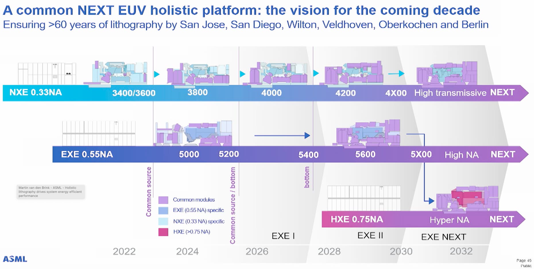
The current 13.5 nm wavelength will likely be used for a while; it is already very close to X-rays. There are some studies where wavelengths lower than 13.5 nm are used, but new problems start to arise there. The printable linewidth can be reduced in two ways: by decreasing the wavelength or by increasing the NA (numerical aperture) of the optics. Currently, ASML and Imec are investing in increasing the numerical aperture of the optics. This also causes power consumption and heat, for which Canatu’s solution is certainly effective.
On ASML’s roadmap, those “High NA” and “Hyper NA” platforms are not very far off, so the need for next-generation pellicles is certainly only set to grow:
A pellicle in a reticle or mask is not a new thing in itself. They have been used for years, and their purpose is to protect the chrome surface of the reticle or mask where the pattern to be exposed is located. As has been noted here, EUV sets new requirements for pellicles, such as heat resistance and filtering.
ASML has completed its High NA machine. A stepper with a higher numerical aperture is by no means a given. The larger the optical aperture, the more the optics’ DOF (Depth of Focus) decreases. In lithography, the device’s DOF is extremely important; the higher the DOF, the better the device tolerates errors such as uneven resist application. The physical dimensions of the mirrors used to guide the light to the reticle also increase due to the higher aperture. Additionally, ASML High NA optics have an 8x reduction in one direction and 4x in the other. Hyper NA is still a long way off, but it’s surely coming at some point, as long as fundamental problems can be solved ![]()
Going slightly off-topic!
A few thoughts based on the materials and the CEO’s video:
Company Facts
Thoughts
Business Case:
Assumption:
It’s great, in itself, that we are getting a growth company on the stock exchange that also has good margins and a growth trajectory. Good luck to the investors and management.
I’ll challenge this a bit: is there any other source for this besides the company’s presentation slides? ![]()
The company doesn’t actually disclose its actual customers (or their number), but lists potential customers. So, there could be significantly more, or significantly fewer. If there’s a reason for more detailed conclusions, I’d love to hear it!
Otherwise, good points!
I think it’s truly great that we have these kinds of innovative and high-tech budding growth companies in Finland. As an investor, quite frankly, this is too challenging a case for me, as I lack any expertise or insight into the technology in this field, let alone its future prospects. I don’t believe that by reading the company’s presentations I could delve deep enough into the subject to even claim to myself that I understand it.
However, I tip my hat to those retail investors who dare to put their money into these, based primarily on the claims of salespeople. Sometimes risk-taking is rewarded handsomely, but the average success rate is likely in the single digits. The valuation doesn’t seem particularly attractive to me either, so I’ll gladly leave these millions for others to reap.
You can get a pretty good idea of how the technology works from here: Electrochemical detection with carbon nanotubes . Meaning flawless (?) or pristine carbon nanotubes with a larger surface area = higher sensitivity. The Theranos case has probably pissed in the cereal of quite a few medical device startups.
There are also many academic publications supporting the sensitivity story (apparently a more limited selection chosen here: Latest research on electrochemical biosensors using Canatu CNT - Canatu ). But indeed, the mentioned cancer detection, for example, cannot be found in any publication.
Revenue development is not linear for this type of company, as is also evident from the materials. According to the company, developing and scaling the technology to an industrial scale takes 15+ years. There is a long journey of development work and a large amount of investment behind them. These naturally weigh on profitability while the scaling of revenue is still in progress.
Why would it be worth limiting the utilization and sale of the technology to just two segments? Especially since the company has just secured significant funding. Surely that, if anything, ensures sufficient resources.
On competitive advantages: the company stated that their process is two-stage and significantly more efficient than those of their competitors. Competitors’ processes involve 8+ stages.
I understand the doubts, but I believe the company has already addressed many of these points at this stage.
The company’s 100 million revenue target for 2027 is already quite close in terms of timing. In my opinion, this is positive in the sense that the company must be able to deliver strong growth figures this year and next for the 2027 targets to be realistic. So, we won’t have to wait long to see how this plays out.
Canatu’s CEO says at least that Canatu’s way of manufacturing carbon nanotubes is unique and a completely different approach from other competitors. It wasn’t quite clear what the actual competitive advantage relates to: are Canatu’s carbon nanotubes better in terms of cost competitiveness because of the different manufacturing method? Or is the power consumption lower with Canatu’s tubes? At least from the CEO’s speech, one gets the impression that the competitors’ way of manufacturing is more cumbersome and not as precise/specific as Canatu’s, which could indicate at least cost competitiveness.
Does expert @Pandakarhu have any insights on this?
The analysis missed the mark there, as you assumed that the potential customers in the image are already existing customers.
Additionally, the semiconductor industry has only taken off very recently. When Lifeline first examined Canatu, that semi side was practically absent from the customer base (almost exclusively automotive sector customers, led by Denso).
The valuation is in line with semiconductor valuations, where EV/S >10 is quite normal. Those Japanese competitors, who manufacture using different methods (a chemical industry approach), are not relevant peers in terms of valuation as they are chemical industry conglomerates; Mitsui, for example, has 181 products:
And those competitors (Mitsui, Lintec) are still at the starting blocks regarding CNT.
At the end of May, news came out that Mitsui is establishing CNT facilities (the CEO also referred to this in his presentation; CNT stands for carbon nanotube):
Canatu explains their view of the competitive advantages of their process in more detail on their website:
I suspect there will be a foreign acquisition offer for Canatu in less than two years, because that technology can easily generate tens of billions.
By that logic, no nanotechnology solution would be worth patenting. Material properties can indeed be tested. If Canatu, on the other hand, were a company making server-side software, patent infringements would be significantly harder to detect.
Here is an example of a patent granted to Canatu, which is still valid for about 10 years:
https://patents.justia.com/patent/10718503#claims
Sample of an independent claim:
a flexible and formable light-emitting active layer;
two conductive or semi-conductive electrodes positioned on each side of the active layer, wherein at least one electrode is transparent and comprises at least one of the following: HARM-structures (High Aspect Ratio Molecular structures), Mono-Crystalline Surface (MCS) structures, conductive or semiconductive polymers, weaved metal fabric and a metal mesh; and
at least one touch sensitive region, wherein the touch sensitive region comprises at least one of the following:
a touch sensitive region in at least one of the conductive or semi-conductive transparent electrodes, and
one or more layers of flexible and formable touch sensitive material,
wherein the light-emitting film is configured to wrap around a complex three-dimensional surface.
————-
Proving such an infringement should not be at all impossible.
“Competitive advantage / or the threat of new products is difficult to assess. Based on a gut feeling, patents might not help much when detecting patent infringement is at the nano-level.”
just a gut feeling