The patent describes how magnetic frame assembly used to attach the pellicle to the photomask.
It would refer more to the frame, rather than the pellicle film itself.
It has not been registered. It is the first patent that S&S Tech filed with another company.
At least I couldn’t find this in a Google patent search, because it was left unregistered? Maybe I didn’t know how to search correctly, but applications should also be found with the correct number…
Samsung currently uses the majority of its EUV blank mask through supplier Hoya of Japan. Through its collaboration with S&S Tech, the South Korean tech giant is aiming to localize some of the EUV blank mask production within the year.
The chip giant is also considering S&S Tech and FST as suppliers for EUV pellicles. Samsung already has a co-registered patent, in 2024, on EUV mask adhesive with FST.
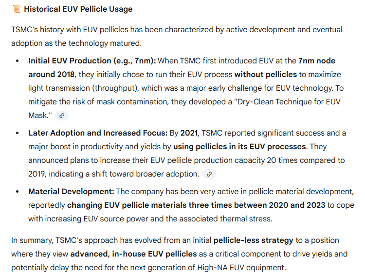
Samsung, despite using ASML’s EUV equipment in its advanced chip production, has so far not used any pellicles during EUV processes.
For months you have been asking on this forum for data that even professional investors don’t see a need for. Understandably, as a pioneer in the field, you are interested in these matters for slightly different reasons than the average investor, but making a fuss about it here will not lead anywhere.
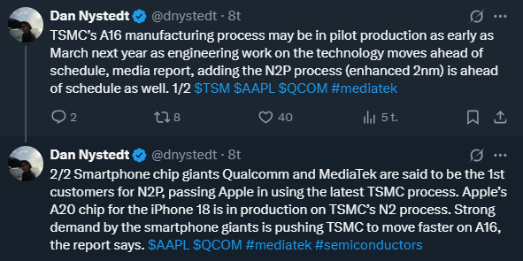
TSMC is thus starting 2nm production by the end of the year and 1.4nm production seemingly in 2028. According to the news below, standard EUV equipment (not High NA) has been acquired for 1.4nm production. The news elaborates on the matter. A large-scale investment, as 30 older devices are being acquired.
TSMC is already moving at lightning speed, with R&D of the 1.4nm process starting at the Hsinchu plant, with the acquisition of 30 EUV machines.
What is interesting for us in the news is the following:
However, one move that TSMC refuses to make is to purchase ASML High-NA EUV machines, which cost $400 million apiece. However, this equipment will ensure the reliability in manufacturing 1.4nm and 1nm wafers at a higher yield. The company likely believes that the dollar value attached to this hardware does not equate to its actual value, which is why, according to Dan Nystedt and Commercial Times, TSMC is moving to photomask pellicles instead. Processes of sub-2nm must have a pellicle in the mix to prevent dust and other particles from contaminating the procedure.
Here are further justifications why pellicles are mandatory with older equipment in the <2nm class:
Again, this is a costly move that is accompanied by a great deal of complications. For instance, when producing 1.4nm and 1nm wafers using standard EUV machines, more exposure will be necessary, meaning that the photomask will be used often to achieve success, which can compromise yields. During this phase, the use of pellicles will be absolutely mandatory to prevent the aforementioned dust particles and contaminants from entering the wafer-manufacturing stage.
From this, one could probably conclude that pellicles will then be mandatory for TSMC starting from 2028. And that ‘whoever offers them pellicles will be happy’?
In the TJ review above, it was also mentioned that 1.6nm would start in H2/2026, but this should be checked. I don’t know if pellicles are mandatory here too. Such a conclusion could be drawn from the aforementioned news.
edit. here also a TSMC roadmap where 1.6nm is in 2026
In my opinion, this news turns positive even though TSMC is delaying high NA investments. With Low NA, multi-patterning must be used, where it is already known that the need for masks is high. Now, to squeeze the last drops of juice from the lemon (low NA), pellicles are adopted in the hope of improving yield.
At the August half-year review press conference, CEO Juha Kokkonen stated, in my opinion, clearly for the first time that pellicles will be used with low NA, which would be in line with the news that @timontti commendably spotted.
If this news holds true, then it could be said that the famous can wasn’t kicked very far down the road if low NA adopts pellicles.
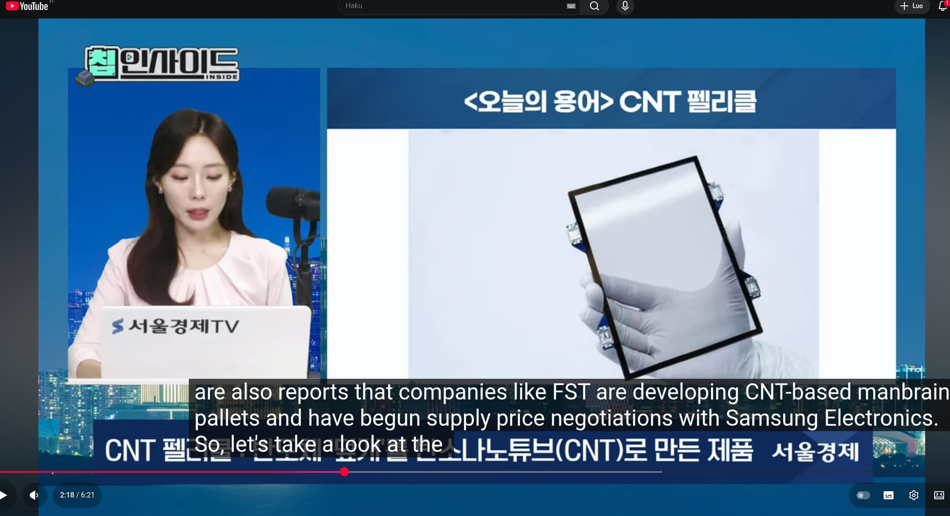
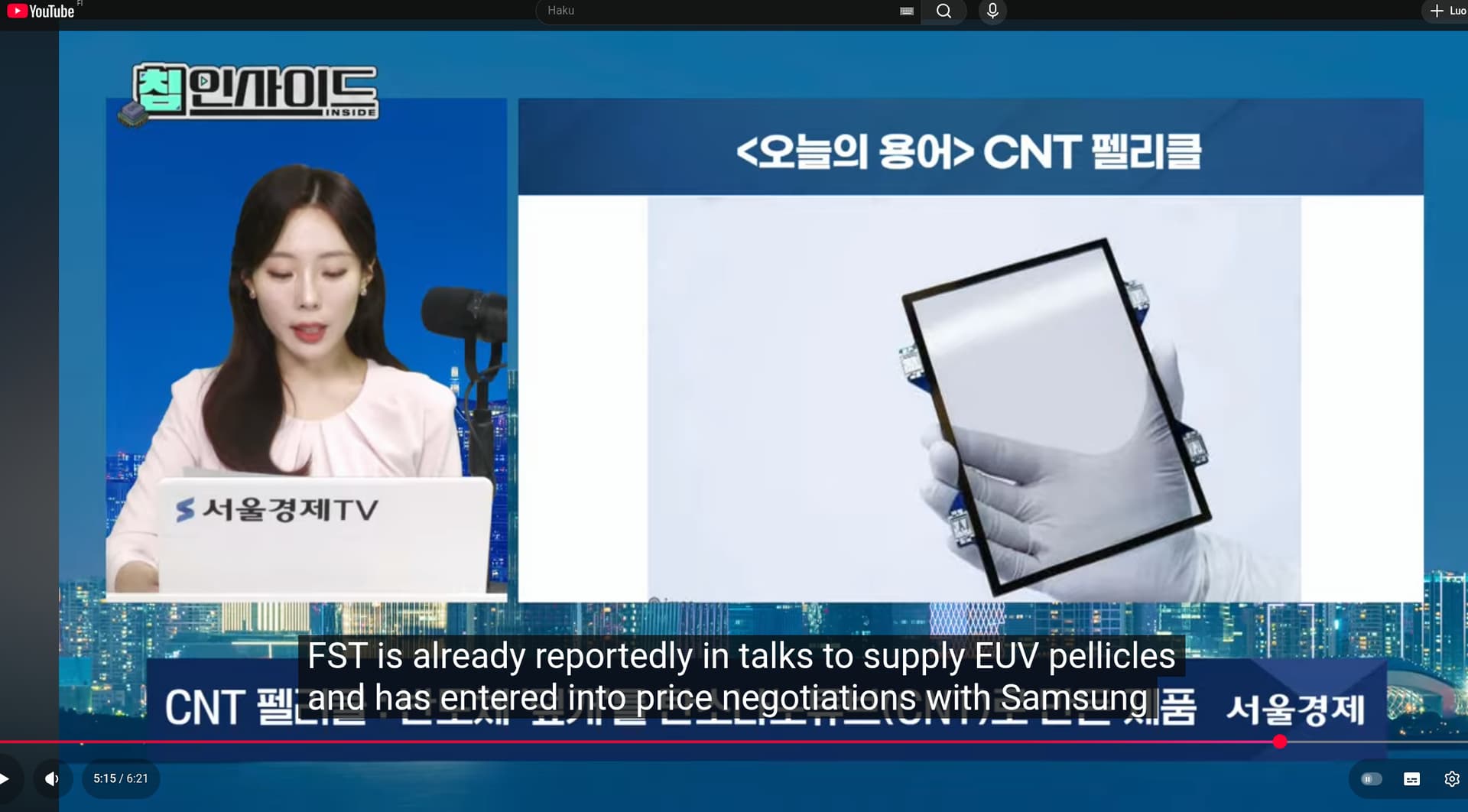
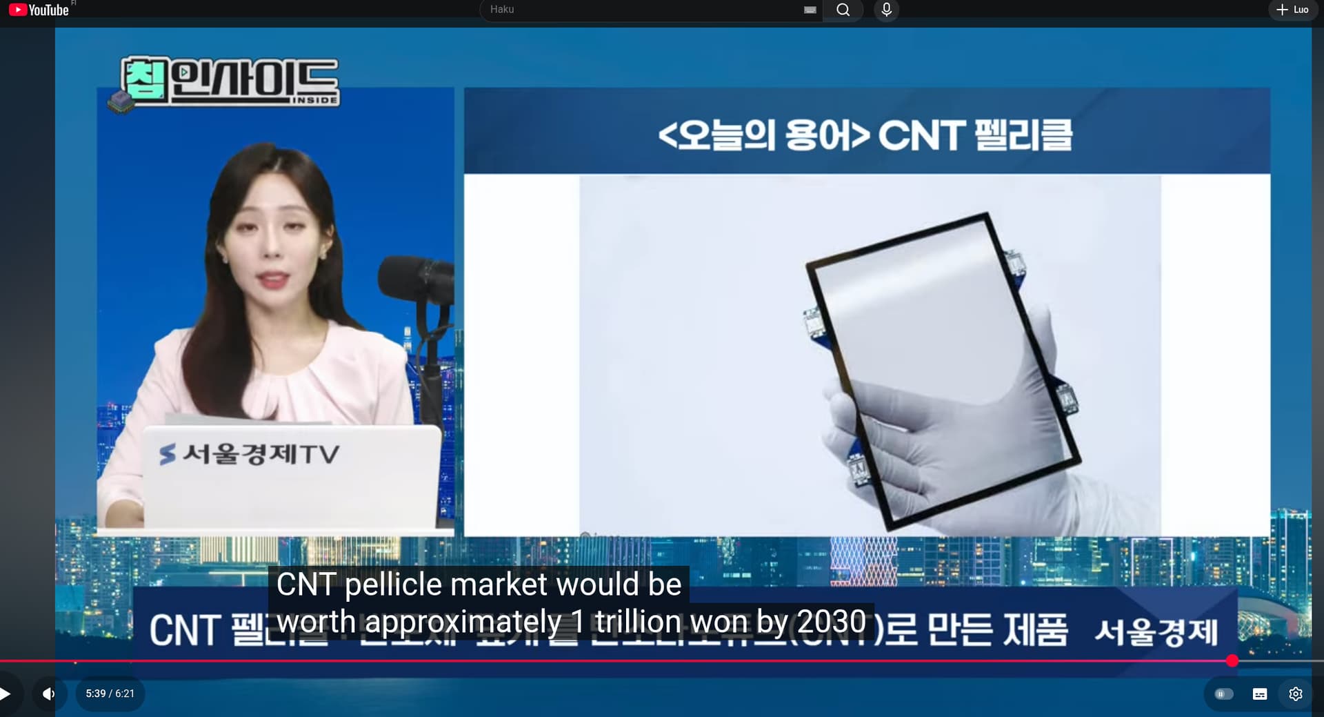
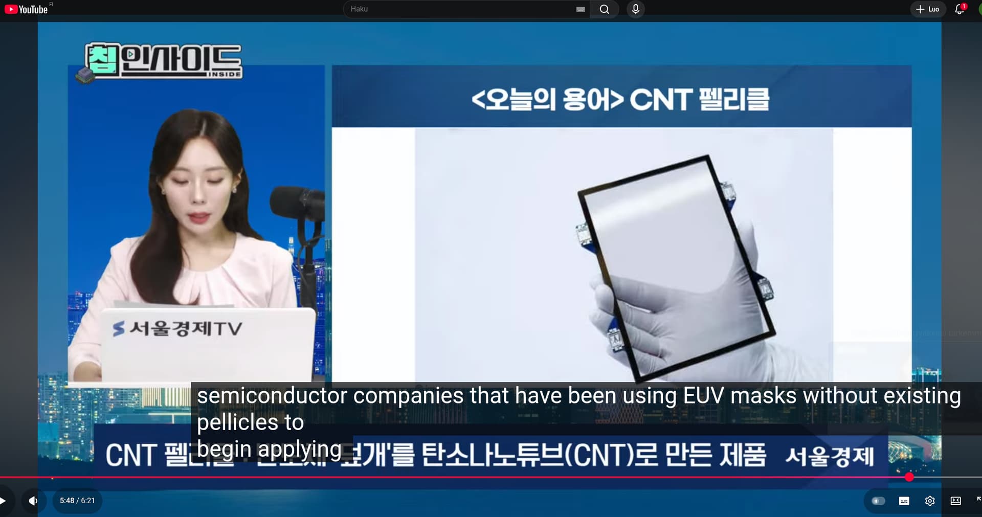
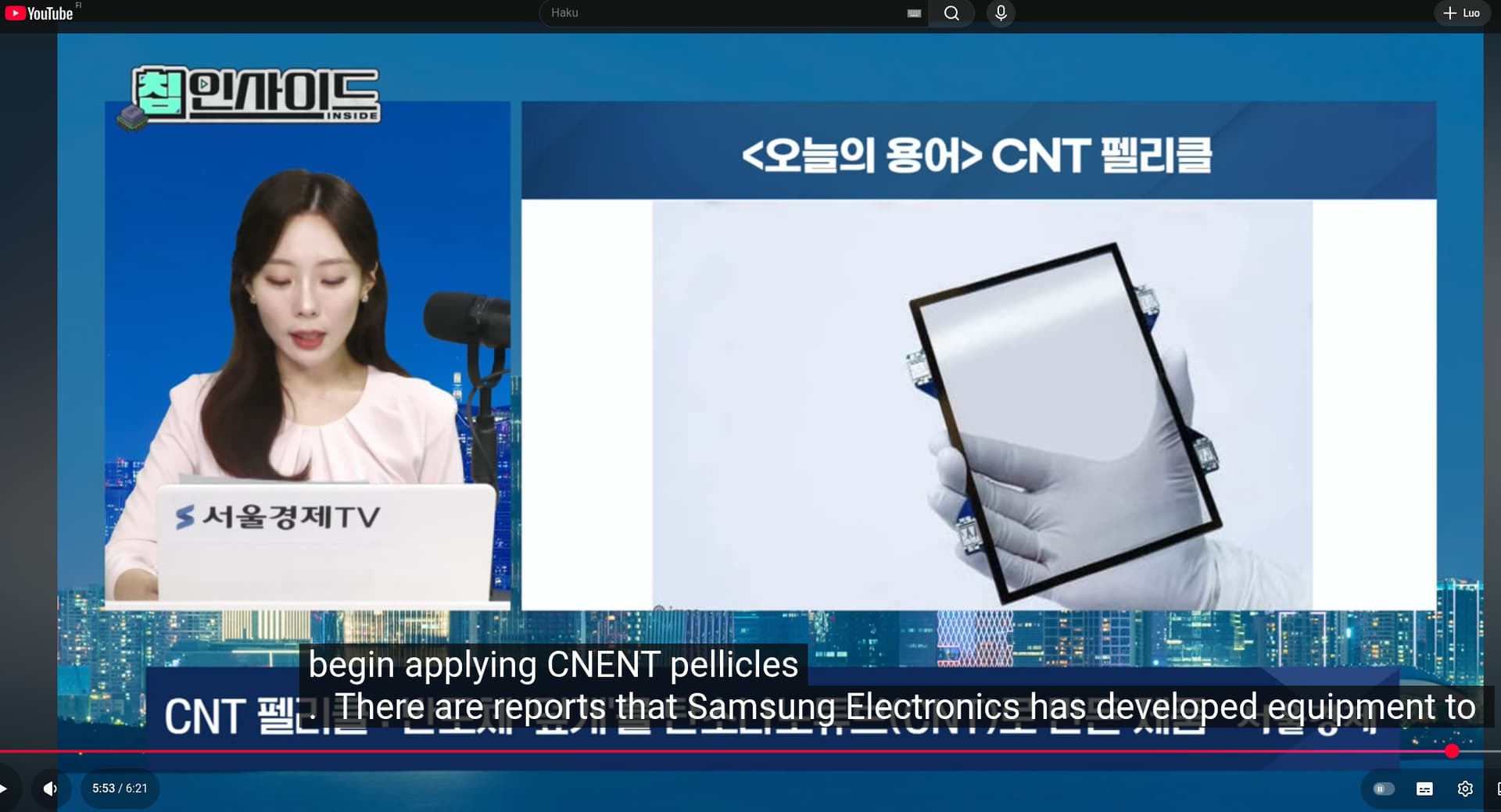
FST-Samsung related content also spotted in this video, when using a translator. The video, as far as I can tell, informs Koreans about EUV Pellicle production.
“The company believes that no other entity than Canatu has sold carbon nanotube reactors for the production of carbon nanotube pellicle membranes for the semiconductor industry.”
A Korean news agency says that FST has developed a CNT EUV pellicle and is now negotiating the price with Samsung. So the product is probably quite ready.
Can these two pieces of information be combined…?
This is not an airtight proof, and I don’t know the situation of Mitsui and partners in detail… but let’s say that “yes” is at least a realistic possibility as an answer to your question?
Yes, and that news image is indeed from Canatu’s website.
Edit: This is heavily speculative, but from my recent rambling in this thread, one could paint a bullish scenario regarding customers, even with a side note like “Dear Santa,… this Christmas I wish for…”
2026 Samsung in production via FST (realistic possibility)
2027 Intel in production with ASML high NA EUV machines, several machines in use (visibility very uncertain)
2028 TSMC in production on 1.4nm line with at least 30 machines (realistic possibility)
Feel free to shoot down these wild speculations, I won’t mind
This news was already mentioned earlier in the thread (message 265), where it is confirmed that FST’s CNT pellicle is made using Canatu’s reactor, meaning all FST and Samsung collaboration projects should also benefit Canatu:
“FST also applied its own proprietary coating technology to protect this CNT membrane from degrading. Finland’s Canatu supplied the equipment used in the CNT membrane synthesis equipment used by FST.
Meanwhile, Samsung is also expected to use FST pellicles for high NA EUV equipment in future chips”
Canatu Grants License for Commercial Production of CNT-Pellicle Membranes with CNT100 SEMI Reactor
Canatu Oyj Press Release October 23, 2025 at 09:00
Canatu has granted a commercial production license for the first CNT100 SEMI reactor to the Korean semiconductor company FINE SEMITECH CORPORATION (“FST”). The license grants FST the right to mass-produce CNT-pellicle membranes using its own CNT100 SEMI reactor. FST will pay Canatu a one-time license fee for the commercial production rights.
The value of the one-time license fee for the commercial production of CNT-pellicle membranes is classified, according to Canatu’s disclosure policy, in the lower half of the medium category (EUR 1.0-5.0 million). The related revenue will be recorded in the fourth quarter of 2025 (Q4/2025).
The start of commercial production also creates two new future revenue streams for Canatu:
Canatu’s own consumables used in the CNT manufacturing process, sold by Canatu
Royalties paid by FST to Canatu for each CNT-pellicle sold to its end customer
There is uncertainty associated with the realization of such future revenue streams, as they inherently depend on FST and its end customers, and are therefore not entirely within Canatu’s control.
Juha Kokkonen, CEO of Canatu Oyj, comments: “This is a significant milestone that brings our customer closer to the mass production of CNT-pellicles. It also confirms the maturity of carbon nanotube pellicle technology and demonstrates the market demand for CNT-pellicles.”
The first CNT100 SEMI reactor was delivered to FST in September 2024. In July 2025, Canatu announced that the reactor and associated post-processing equipment had passed customer acceptance (Site Acceptance Test, SAT). The mass production license now granted is part of the agreed roadmap towards commercial deployment.
Here are also Ate’s comments regarding this recent news.
Canatu announced on Thursday that it had granted a commercial production license for the first CNT100 SEMI reactor to the Korean semiconductor company FINE SEMITECH CORPORATION (”FST”). The license grants FST the right to mass-produce CNT-pellicle membranes using its own CNT100 SEMI reactor. With the announcement, the name of Canatu’s first reactor customer has now also been officially revealed, although based on various news sources, the matter was already known earlier.
An article written on Twitter early this month discusses EUV Pellicle quality inspection from Samsung’s perspective… it doesn’t contain anything new, but it talks a bit about technical features and inspection
TSMC Reportedly Constructing Four Plants For 1.4nm Wafers, Mass Production Happening In H2 2028, A Single Facility Can Bring In $16 Billion Revenue
Risk production at one of the plants is estimated to begin by the end of 2027, with mass production scheduled for the second half of 2028.
What is interesting to note is that the initial $49 billion investment will not be used to purchase any of ASML’s next-generation and expensive High-NA EUV equipment. Instead, TSMC believes it can pursue 1.4nm production without purchasing those $400 million machines and will resort to using photomask pellicles to improve yields.
A follow-up question to that is, with which pellicles can 1.4nm be best produced without High NA EUV equipment? Can we still continue with existing suppliers and pellicles, or will better yield be achieved with Canatu’s products?
In High NA EUV equipment, it was “necessary to switch to better pellicles” so that they physically withstand. Is there such a necessity in this Taiwan Semi scenario?
On the other hand, this recent article from September states, among other things:
Temperatures near 1000 degrees in EUV devices
EUV-pellicle unit price estimate 10k$; to be changed every 3-4 days.
internalizing production → pellicles are produced in-house to be more profitable (would Canatu reactor technology fit?)
This is at least a strong hint: ‘That financial case goes hand in hand with materials research: carbon nanotube membranes are the most promising candidate to meet the twin demands of durability and optical transparency’
Then it refers to “validation of better pellicles in 1.6nm production”.: ‘TSMC plans to validate solutions as it ramps N2 and A16 process technologies, where improved pellicle performance could significantly boost yields and preserve its edge on advanced nodes’
At least from this, one could try to make some kind of deduction:
Moving to in-house production. Higher quality pellicles, over 10x more expensive, are in use. Would these need separate validation if the same ones as before were used?
If ‘old model pellicles’ were suitable for the production of the newest chips, would it then make sense to switch to pellicles that are over 10x more expensive?
Carbon nanotubes mentioned as the material
I myself would assume that Canatu pellicles are likely for 1.4nm production starting from the end of 2027, based on the aforementioned news. On the other hand, the news linked in this post could allow for their use already in 1.6nm production (“validate solutions”). And the screenshot I linked in my previous post indicated that 1.6nm initial production is possible already in March 2026 due to high demand for chips.
If I were a small Finnish deeptech company with management that has good strategic insight, would it be a good time to organize a CMD in March when 1-2 customers are already in production or at least close to it?
Canatulla is a unique growth story on the Helsinki Stock Exchange with the potential to reach the billion-euro class. As the demand for microchips grows rapidly, the company has an opportunity to capitalize on this growth with its carbon nanotube (CNT) reactors and products refined from them.
However, the potential is well known in the market, and investors bear a significant valuation risk in the stock. The company’s EV/Sales ratio, or enterprise value relative to revenue, is as high as 18.8. At this multiple, it would take Canatulla almost 19 years to accumulate its current debt-free value measured by revenue.
Although Canatu’s business is high-margin and its growth prospects are strong, the share price does not include a margin of safety. The delay in reactor approvals has already melted a third off the share price this year, and yet the valuation is not particularly low.
Canatu’s technology currently appears superior, but high-margin business inevitably attracts competitors. It is therefore unclear how long the company’s competitive advantage will last. In addition to the valuation risk, the overall picture is overshadowed by the small number of customers, as the company has only a few global clients.
On the other hand, the company aims to diversify its risk outside the semiconductor sector, for example, into the automotive industry. However, this involves a compromise: margins in automotive applications are unlikely to be higher than in the semiconductor industry, so diversification could erode profitability. Greater potential may lie in early-stage ventures, such as the defense and pharmaceutical industries, where applications could be higher-margin. However, the timeline for revenues generated by these is still completely uncertain.
OCSiAl is the only company with a scalable technology for industrial synthesis of graphene nanotubes
I wonder why different terminology is used in these?
“Graphene nanotubes, or single wall carbon nanotubes, are graphene sheets shaped as a tube.”
Nothing is really said about films/membranes anywhere, so they probably operate in different markets and use a different manufacturing method.
“OCSiAl is not the only company that has appreciated the ability of graphene nanotubes to modify most materials used in industry and everyday life. This is evidenced by the thousands of patents and hundreds of thousands of scientific developments based on nanotubes.”